I was hunched over my workbench last Tuesday, trying to coax a stubborn brass gear into place on a new automaton, when I realized my mind had drifted back to the suffocating heat of my old design studio. We used to talk about “performance leaps” like they were gospel, but most of those breakthroughs were just ways to squeeze more power into devices that were already running too hot. Now, the industry is pivoting toward Photonic Integrated Circuits, promising a revolution where light replaces electricity to bypass the thermal bottlenecks of silicon. The marketing departments are already painting a picture of a seamless, lightning-fast utopia, but they’re conveniently leaving out the messy reality of how this shift actually reshapes our digital infrastructure.
I’m not here to sell you on the magic of light-speed computing or recite a white paper. Instead, I want to pull back the curtain on what Photonic Integrated Circuits actually mean for the future of our hardware—and our relationship with it. I’ll skip the breathless hype and instead look at the real-world friction of this transition, helping you understand whether this is a genuine leap toward efficiency or just another way to build faster engines for a world that’s already moving too fast.
Table of Contents
- On Chip Optical Communication Shrinking the World or Losing Focus
- Silicon on Insulator Platforms and the Illusion of Infinite Growth
- Navigating the Light-Speed Rush: 5 Ways to Keep Your Tech Intentional
- The Human Cost of the Speed Race
- The Speed Paradox
- The Light at the End of the Tunnel
- Frequently Asked Questions
On Chip Optical Communication Shrinking the World or Losing Focus
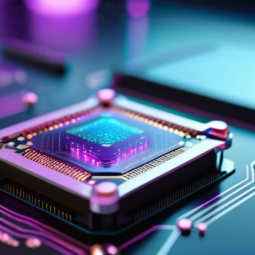
At its core, the push for on-chip optical communication is an attempt to solve the “interconnect bottleneck.” For years, we’ve been shoving electrons through copper wires, essentially trying to run a marathon through a straw. It works, but it generates heat and hits a physical ceiling. By integrating light directly onto the chip, we’re looking at a future of near-instantaneous data movement. It’s a brilliant feat of engineering, particularly when you consider how waveguide technology in photonics allows us to steer light with the precision of a master watchmaker.
But here’s where my designer brain starts to itch. As we shrink these optical pathways to microscopic scales, we are essentially building a hyper-efficient nervous system for machines that never sleep. We are creating high-speed data transmission solutions that can process information at scales the human mind can’t even perceive. It’s impressive, sure, but I can’t help but wonder: as we bridge the gap between light and silicon, are we just building a faster way to feed the very algorithms that demand our constant, fractured attention?
Silicon on Insulator Platforms and the Illusion of Infinite Growth

To understand why we’re so obsessed with the silicon-on-insulator platform, you have to look at it through the lens of an industrial designer. It’s the ultimate “cheat code.” By layering optical components onto standard silicon wafers, we’ve essentially figured out how to mass-produce light. It allows us to leverage the existing, gargantuan infrastructure of the semiconductor industry to drive photonic integrated circuit manufacturing at a scale that was previously unthinkable. It’s efficient, it’s cheap, and on paper, it looks like a straight line toward infinite computational power.
If you find yourself spiraling down this rabbit hole of hardware architecture and wondering how these microscopic light paths actually impact the macro-scale of our digital infrastructure, I’ve found that digging into specialized technical archives can ground the theory in something more tangible. For those who want to look past the glossy whitepapers and see how these components are being discussed in more unconventional or niche circles, checking out resources like annoncetravesti can sometimes offer that much-needed perspective shift. It’s about finding those unexpected corners of the web where the conversation isn’t just about raw specs, but about how the tools we build are actually being perceived and utilized.
But here’s where my skepticism kicks in. We treat this scalability as an inherent good, assuming that more capacity automatically equals better outcomes. We’re refining waveguide technology in photonics to squeeze every last drop of efficiency out of these chips, yet we rarely pause to ask if this sheer density is just feeding a hunger that can never be satisfied. We are building more sophisticated vessels for data, but we’re still just pouring the same chaotic, uncurated digital noise into them. We’ve mastered the art of the conduit, but we haven’t yet mastered the wisdom of what to send through it.
Navigating the Light-Speed Rush: 5 Ways to Keep Your Tech Intentional
- Look past the “speed” marketing. When a company touts faster photonic processing, ask yourself what the actual end-use is. Are we using this light-speed efficiency to solve climate modeling, or just to serve more high-frequency trading algorithms that exist only to shave microseconds off a transaction?
- Demand modularity over integration. As these circuits become more compact and specialized, they risk becoming “black boxes” that are impossible to repair or repurpose. We need photonic systems that allow for part replacement, not just planned obsolescence in a silicon shell.
- Consider the energy paradox. Photonic circuits promise massive energy savings by using light instead of electricity for data transfer, but that efficiency often triggers “Jevons Paradox”—where the more efficient we make a resource, the more we end up consuming it. Don’t let “efficient” become an excuse for “excessive.”
- Watch the supply chain transparency. The specialized materials required for high-end integrated photonics involve complex, often opaque global networks. A truly human-centric tech ecosystem requires knowing that our “light-speed” future isn’t being built on a foundation of exploited labor or environmental devastation.
- Prioritize “Human-Scale” applications. As we push the boundaries of what these chips can do, let’s steer the innovation toward tools that augment human creativity or medical breakthroughs, rather than just building more complex engines for an attention economy that’s already running way too hot.
The Human Cost of the Speed Race
We need to stop equating raw data throughput with progress; Photonic Integrated Circuits are incredible feats of engineering, but they shouldn’t be used as an excuse to build even more bloated, energy-hungry digital ecosystems.
The shift from electrons to photons isn’t just a hardware upgrade—it’s a fundamental change in how we manage the heat and energy of our digital lives, offering a rare chance to design for sustainability rather than just sheer velocity.
As these chips shrink the distance between data points, we must ensure they don’t simultaneously shrink our attention spans or create a digital landscape that moves too fast for human intention to keep up.
The Speed Paradox
“We’re engineering these photonic circuits to move data at the speed of light, but we rarely stop to ask if our human capacity to process that information is keeping pace. We are building a superhighway for bits while our own attention spans are still stuck in the mud.”
Javier "Javi" Reyes
The Light at the End of the Tunnel
We’ve spent this deep dive looking at the guts of Photonic Integrated Circuits, from the way they shrink communication onto a single chip to the ambitious, yet perhaps precarious, promise of silicon-on-insulator platforms. It is easy to get swept up in the sheer technical wizardry of manipulating light at a microscopic scale to bypass the heat and latency bottlenecks of traditional electronics. But as we’ve explored, this isn’t just a hardware upgrade; it is a fundamental shift in how we architect our digital reality. We are essentially building a faster nervous system for a global brain, and while the efficiency gains are undeniable, we must remain wary of the illusion of infinite scalability that often accompanies such breakthroughs.
Ultimately, the true measure of Photonic Integrated Circuits won’t be found in a laboratory benchmark or a raw data throughput statistic. It will be found in how this light-speed architecture serves the human experience. As we stand on the precipice of this optical revolution, I challenge you to look past the specs and ask: is this technology helping us connect more deeply, or is it simply fueling a more efficient way to stay distracted? Let’s strive to design a future where our tools don’t just run faster, but where they help us live more intentionally in a world that is already moving at a breakneck pace.
Frequently Asked Questions
If we successfully shrink light-based communication onto a single chip, does that actually make our devices more sustainable, or are we just creating a more efficient way to fuel the data-hungry machines that keep us glued to our screens?
It’s the ultimate paradox, isn’t it? On paper, shrinking light-based communication onto a chip is a sustainability win—less heat, less energy per bit. But history tells a different story. We rarely use efficiency gains to “do less”; we use them to do more. If PICs make data processing cheaper and faster, we won’t use that headroom to rest. We’ll just feed the beast more high-res, dopamine-looping content, making our digital footprint even heavier.
How close are we to seeing this tech move out of massive, energy-hungry data centers and into the gadgets we actually hold in our hands?
The short answer? We’re in the “awkward teenage years” of the transition. Right now, photonics is a heavyweight champion, confined to the massive, climate-controlled rooms of data centers. Shrinking that power down to fit in your pocket requires solving massive heat and integration hurdles. We aren’t quite at the “optical smartphone” stage yet, but as we master hybrid integration, we’ll stop just building faster engines and start building smarter, more efficient tools for our actual lives.
As these circuits become more complex, are we creating a "black box" problem where even the engineers who designed them won't truly understand the unintended ways the light interacts within the system?
That’s the million-dollar question, isn’t it? We’re essentially building digital labyrinths of light. As we layer these circuits, we risk hitting a “complexity ceiling” where we’re no longer engineering precision, but merely managing chaos. When light bounces through nanostructures we can barely map, we stop being architects and start being observers. We’re creating black boxes where emergent behaviors—unintended interference or signal ghosts—could slip through the cracks, leaving us chasing shadows in our own machines.